


The GPU Tsunami framing recap: The race to accelerated computing, driven by AI workloads and the GPU, is pulling forward the entire semiconductor ecosystem as the industry races to meet demand, develop significantly more advanced chips, and solve new engineering challenges which emerge.
For most of the semiconductor industry’s history, test followed a familiar flow around a mostly monolithic chip. The angstrom era is changing that as chiplets, HBM, and other disaggregated designs turn the finished device into a system assembled from several pieces. Every additional die and connection creates another place a defect can appear, while more value is committed before final test. This is forcing manufacturers to screen earlier and add checks after assembly, often under harder power and thermal conditions.
A year ago, all major semiconductor companies told us testing would play a larger role as design complexity increased. We sat on this report because we were unsure how far into the manufacturing flow to take readers. Recent earnings make the change visible across the test market and we think tracking the category shows some early design signals worth playing attention. We are tracking the main test suppliers because each gives us a signal from a different part of the market. Aehr shows where wafer-level burn-in is moving into production. Teradyne and Advantest show how functional-test time and equipment demand are changing across advanced compute and memory. Cohu shows where hotter, more complex packages require new handling, thermal control, and inspection. Together, they reveal where rising design complexity is turning into additional factory work and test capacity.
The GPU Tsunami is reaching semiconductor test
Semiconductor manufacturers use test machines, commonly called testers, to apply power and signals to a chip and confirm that it works. Each machine has a fixed number of hours available. Larger accelerators can remain on the machine longer because they draw more power and require deeper test patterns, reducing the number of chips each tester can process. Advanced packaging adds cost around every die, while optical I/O introduces checks that can only happen after more of the device has been assembled.
We therefore focus, and have framed an economic model, on test content per sellable AI system: the total factory work required to prove that the components and the completed system will operate as intended. Chip volume remains important, although it is only one source of demand. Test capacity also grows when a device occupies the machine longer, requires checks at additional manufacturing stages, or consumes enough power that fewer devices can be tested at once.
Required test capacity = unit volume × test insertions × test seconds per insertion ÷ effective parallelism
Each part of the model has a direct meaning. More devices, additional checks, and longer tests increase the equipment requirement. Testing more devices at the same time reduces it.
In the full report, we use this model to estimate where the added test value can accrue. Functional-test suppliers benefit when processors require more machine time. Handling and optical-test companies participate when advanced packages create new checks. Wafer burn-in depends on how many wafers receive sustained stress and how long the process takes. We then map that capacity to equipment content and supplier position to estimate the commercial opportunity.
Wafer burn-in finds weak die before they become expensive failures
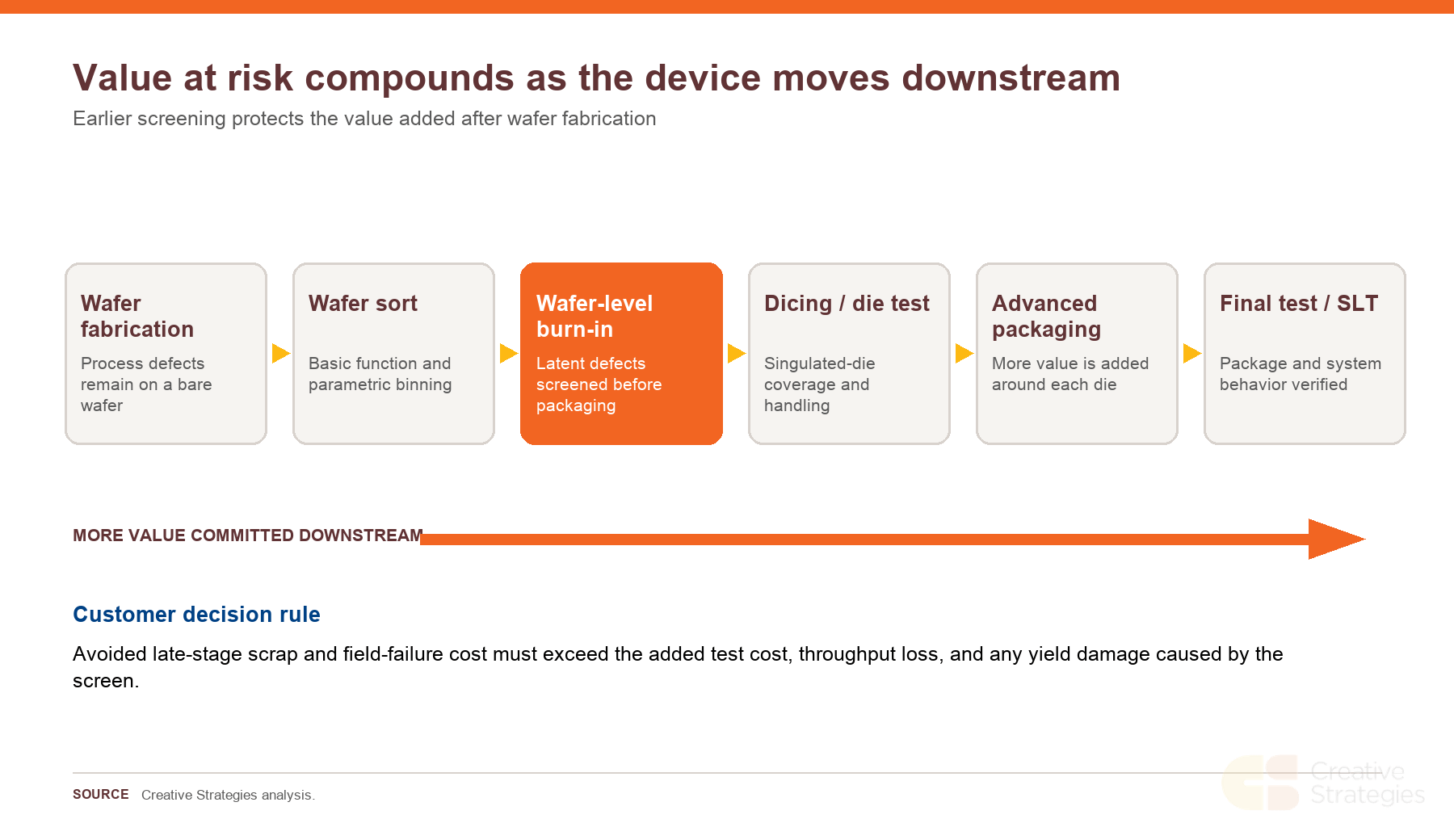
An individual chip, called a die, can pass a short electrical test and still carry a weakness that appears only after sustained heat or power. An AI accelerator die, as an example, can pass a short electrical test while still carrying a weakness that appears only after sustained power and heat. If the failure is discovered after the processor has been packaged with HBM, an interposer, and other components, the manufacturer can lose the value of the entire assembly. Wafer burn-in applies that stress before the expensive package is built.
Finding the weakness at this stage lets the manufacturer remove the die before packaging. A failure discovered later can destroy the package, the good die inside it, and the work already used to assemble everything. Earlier reliability screening protects more value as the package becomes more expensive.
To show how the risk compounds, assume a package requires eight to twelve die and that each selected die has a 98% to 99.5% probability of being good after screening. If failures are independent, the probability that every required die is good ranges from approximately 78% to 96% before assembly losses. These are illustrative assumptions, not measured industry yields. The point is the multiplication: as packages combine more required die, even a small improvement in die-level confidence can protect substantially more downstream value.
Test orders show where advanced silicon is entering production
Recent earnings put numbers around this functional change for testing. Our blended measure of broad automated-test revenue grew roughly 35% to 45% in the latest full-year periods. More recent disclosures show compute-related test revenue and orders rising roughly 100% to 150% year over year. A separate test-cell utilization series moved from the mid-70% range to about 80%.
Wafer burn-in adds a specialized production indicator. Effective backlog at one supplier is roughly twice its recent annual revenue, supporting a forward revenue range of about 2.5 to 3 times that base. These figures measure different jobs and periods, so we treat them as independent markers of customers committing more factory time and equipment to advanced silicon.
Test equipment can reveal where a new chip architecture sits in the manufacturing cycle. An engineering system shows that a chipmaker has reached a new test problem. Qualification shows that the equipment can find a failure or performance limit the customer cares about. A production installation means the test has cleared the cost and throughput hurdle required to become part of manufacturing. Repeat orders show that the program is scaling or that the same test is spreading to more devices.
We highlight Aehr here because our conviction is it gives us a tangible view of that progression because its system configuration and order pattern reveal how customers are using wafer-level burn-in. Silicon carbide established the production case, while recent repeat capacity for AI processors and silicon photonics shows the process moving into additional high-value manufacturing flows. We apply the same framework across the broader test market to interpret functional-test, handling, optical-test, and reliability-equipment demand.
Inside the full report
An original capacity model showing how more test steps, longer test times, and parallelism translate into equipment demand across the test market.
A manufacturing-flow map showing where test enters accelerators, HBM, advanced packaging, and optical I/O.
A wafer-burn-in sensitivity model that converts screening coverage and stress time into required production capacity.
An application map separating current production evidence from the next proof point across SiC, silicon photonics, GaN, silicon power, advanced packaging, and memory.
A value-capture map showing which suppliers participate in each test job, how the spending reaches them, and what evidence to track.
A monitoring ladder that follows new test processes from engineering and qualification through factory transfer, repeat capacity, and adoption across independent programs.
Yesterday we introduced CS Atlas, a new research platform from our firm Creative Strategies, now available to all current subscribers. Use it alongside this report to go deeper into the work behind our view—from the signals across Aehr, Teradyne, Advantest and Cohu to the links between semiconductor test, advanced packaging, HBM, optical I/O and power semiconductors. Atlas can help you compare suppliers, work through our capacity model and identify when a new test process is moving from engineering into production.Some suggestion prompts for CS Atlas on this subject:
“Compare the demand signals provided by Aehr, Teradyne, Advantest, Cohu and FormFactor.”
“How do chiplets, HBM and advanced packaging increase test content per sellable AI system?”
“What milestones show that a test process has moved from engineering to qualification and production?”
“Where does wafer-level burn-in have the strongest technical and economic fit across SiC, GaN, silicon photonics, advanced packaging and memory?”
“How does optical I/O change the number and type of tests required during manufacturing?”
“Which assumptions have the greatest effect on required test capacity: units, test insertions, test time, parallelism or screening coverage?”
